|
SEM - EDS
|
|
| |
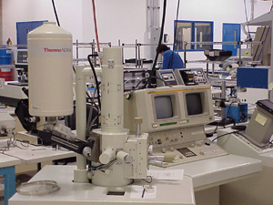
Scanning Electron Microscopy (SEM)
|
|
| |
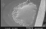
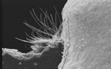
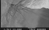
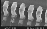
A scanning electron microscope is used to determine the topographical
image or make-up of a sample. It has a greater depth of field, higher resolution
and higher magnification than an ordinary optical microscope. It is relatively
easy to use and is widely-used in almost all research areas. The SEM only produces
high-resolution images of the sample surface. Therefore, the internal structures
of the sample cannot be determined unless a
cross-section is performed.
|
|
|
|
| |
Energy Dispersive Spectroscopy (EDS)
|
|
| |
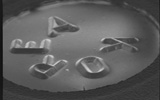
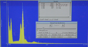
Energy Dispersive Spectroscopy (EDS) is a standard method of
identifying and quantifying elemental composition of sample surfaces. The characteristic
x-rays are produced when the sample is bombarded with electrons in an electron
beam instrument such as a scanning electron microscope. Detection of these
x-rays and discrimination of the x-ray energies can be accomplished by an energy
dispersive spectrometer.
Suspect Pure Tin on the surface of your part? EDS can
validate your suspicion.
|
|
|
|
| |
Applicable Specifications & Standards:
- ASTM E1829, Standard Guide for Handling Specimens
Prior to Surface Analysis
- ASTM E1508, Standard Guide for Quantitative Analysis
by Energy-Dispersive Spectroscopy
|
|