|
Back End Services
|
|
|
|
|
|
Tape and Reel
|
|
|
Tape and reel is the process of sealing components into a carrier
tape for transport and storage. The tape is embossed (vacuum-formed) to safely
hold most types of components. Many of the PCB assembly machines are tooled
to automatically remove the component from the tape and place them on the PCB
for final assembly. This eliminates any manual handling during PCB assembly
and provides a very efficient and safe method of handling.
|
|
|
|
|
Applicable Specifications & Standards:
-
EIA-481
8 mm through 200 mm Embossed Carrier Taping and 8 mm & 12 mm Punched Carrier
Taping of Surface Mount Components for Automatic Handling
|
|
|
|
|
|
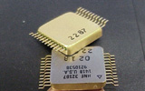
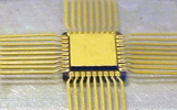
Trim and Form
|
|
|
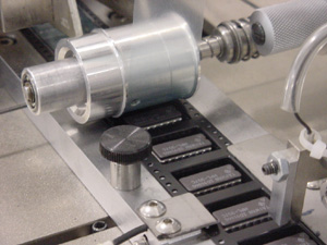
SIX SIGMA has specialized expertise in trim and form of hermetic
glass-sealed components. Trim and Form is the process of cutting and forming
the leads of the component. At SIX SIGMA, components are typically received
in flat-pack format after electrical test then trimmed and formed prior
to hot solder dip (HSD). The HSD process
removes the gold finish which would otherwise cause embrittlement of the solder
joint.
|
|
|
|
|
|
|
|
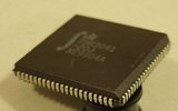
Bake and Dry Pack
|
|
|
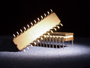
SIX SIGMA offers Bake and Dry Pack to eliminate the moisture
that can damage the components. The process is performed by baking the components
at specified temperatures and times to remove moisture. The components are then
vacuum packed in a special moisture-resistant bag. This process is strongly
recommended for any plastic component that would absorb moisture in storage minimizing any delamination issues when mounting the component to the PC
Board. Components that are vacuum packed can be stored in normal room conditions.
|
|
|
|
|
Applicable Specifications & Standards:
-
IPC/JEDEC J-STD-033
Handling, Packing, Shipping and Use of Moisture/Reflow Sensitive Surface Mount Devices
|
|
|
|
|
|
Physical Dimension Verification
|
|
|
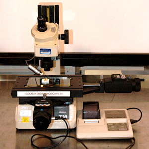
SIX SIGMA utilizes the toolmaker’s microscope, the optical comparator,
and other high-resolution instruments (calibrated and traceable to NIST standards)
to verify that the component’s external physical dimensions are in conformance
with the pertinent procurement document. These instruments are employed for
this non-destructive test, and can be used to evaluate lot acceptance, process
monitor, and qualification.
|
|
|
|
|
Applicable Specifications & Standards:
|
|
| |
|
|
|
|